Introduction
The first amorphous silicon layers fabricated were reported in 1965 the fabrication form was film of “silicon from silane” deposited in a radio frequency glow discharge [1]. Nevertheless, is took more than ten years until Spear and LeComber, scientists from Dundee University, proved that amorphous silicon had semiconducting properties; that is by showing that amorphous silicon could be doped n-type and p-type simply by adding phosphine or dibborane to the glow discharge gas mixture, respectively [2]. This was a far-reaching discovery until that time it had been generally thought that amorphous silicon could not doped. At that time it was not recognized that hydrogen played an important role in the newly made amorphous silicon doped films. In fact, amorphous silicon was suitable for electronic applications, where doping is required, is an alloy of silicon and hydrogen. The electronic-grade amorphous silicon is therefore called hydrogenated amorphous silicon (a-Si:H).
The successful doping of amorphous silicon initiated a tremendous in this material and research activities in this field grew explosively all over the world. There were two main reasons for this interest. First, the material had several interesting properties that opened many opportunities for semiconductor device applications. Second, the glow discharge deposition technique enabled the production of a-Si:H films over a large area and at a low temperature. At present, this material is for instance used for photoconductive layers in electrophotography, for thin film transistors, and not in the least for solar cells.
Due to high absorption coefficient of a-Si:H in the visible range of the solar spectrum, 1 micrometer (µm) thick a-Si:H layer is sufficient to absorb 90% of usable solar light energy. Low processing temperature allows using a wide range of low-cost substrates such as glass sheet, metal or polymer foil. These has made a-Si:H a promising candidate for low-cost thin-film solar cells.
The a-Si:H solar technology has improved tremendously, leading to present solar cells with initial efficiencies exceeding 15% [3]. Today amorphous silicon solar cell technology is matured thin-film solar cell technology that delivered in 2002 a-Si:H modules with the total output power of 35.8 MWp. This represented about 6% of the total PV module production in the world. Recently, experimental modules have been introduced which are based on a combination of a-Si:H solar cell and hydrogenated microcrystalline silicon (µc-Si:H) solar cells, a newly called hydrogenated nanocrystalline silicon (nc-Si:H) solar cells [4].
Hydrogenated microcrystalline silicon deposited using the low-temperature plasma-enhanced chemical vapor deposition (PECVD) technique emerged in this period as a new candidate for the low band gap material in multi-junction a-Si:H based solar cells. The University of Neuchatel introduced a micromorph tandem solar cell in 1994, which comprised an a-Si:H top cell and a µc-Si:H bottom cell [5]. A promising potential of the micromorph cell concept was soon demonstrated by fabricating micromorph tandem and triple solar cells with stabilized efficiencies in range of 9.3 to 10.6 % [6].
Polymorphous silicon thin-films
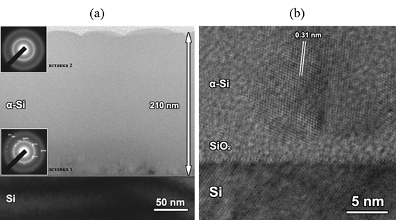
Polymorphous silicon material appeared in 2000 in order to improve the properties of a-Si:H [7]. In 2014 was conducted research at Saint Petersburg Electrotechnical University «LETI» carried in the Department of quantum electronics and optoelectronic devices to improve photoconductivity for a-Si:H thin-films. Increase ratio of hydrogen with increasing pressure in the deposition process has been obtained polymorphous silicon material. The results of scanning electron microscope proved that amorphous silicon films containing Nano-crystalline granules (figure 1) [8, 9].

Figure 1. The image of polymorphous silicon thin-films by scanning electron microscope
(a) Cross-sectional view of the film Pm-Si: H on the silicon substrate. Inset 1 — electron diffraction pattern from the bottom layer α-Si. Present diffraction reflexes from the silicon substrate and of crystalline particles in the bed. Inset 2 — diffraction pattern from the top: visible only diffuse rings corresponding to the amorphous phase.
(b) Image of silicon nanocrystals in the lower part of the layer near the interface with the substrate. The interlunar spacing in the particle match interplanar spacing of crystalline silicon
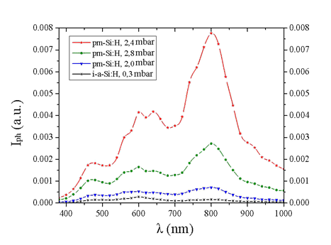
Analysis of the spectra of the photosensitivity films pm-Si:H (figure 2), obtained at different pressures showed that the photosensitive film pm-Si: H, deposited at a growth chamber pressure of 2.4 mbar is highest photosensitivity, which is almost two orders higher than the photosensitivity of the film a-Si: H, precipitated by basic mode.

Figure 2. Spectra photosensitive film a-Si: H, obtained in basic mode, and films pm-Si: H, obtained at different pressures in the growth chamber
It has been found that films pm-Si: H have a number of pronounced maximum near 480, 625 and 800 nm. It proposed the following interpretation of the appearance of these maxima: maximum near 800 nm, determines the presence of the nanocrystalline phase, the maximum near 625 nm, determines the presence of an amorphous phase of silicon with a low content of hydrogen (the part of the film from the free surface) and a maximum near 480 nm, determines the presence of an amorphous phase of silicon with a high hydrogen content (area film from the substrate side).
The appearance of these peaks in the photoconductivity spectra of undoped films of a-Si:H, obtained at high dilution of the silane in hydrogen and containing nanocrystalline incorporation due to a no uniform distribution of hydrogen by volume films a-Si:H, and the presence of high concentrations of a nanocrystalline phase near the interface with the substrate. The results are tested at conferences [8,9].
References:
[1] H.F. Sterling and R.C.G. Swann, Solid-State Electron. 8 (1965) p. 653-654.
[2]W. Spear and P. LeComber, Solid State Comm. 17 (1975) p. 1193-1196.
[3] J. Yang, A. Banerjee, K. Lord, and S. Guha, Proceedings of the 2nd world conference and Exhibition on Photovoltaic Solar Energy Conversion, Vienna, Austria, July 6-10, 1998, p. 187-189.
[4] V.S. Cristobal, Thin film nanocrystalline silicon solar cells obtained by hot-wire CVD. UNIVERSITAT DE BARCELONA, Brcelona (2001).
[5] J. Meier, S. Dubail, R. Flückiger, D. Fischer, H. Keppner, A. Shah, in Proceedings of the 1st World Conference on Photovoltaic Energy Conversion (1994), p.409-412.
[6] Афанасьев В. П., Теруков Е. И., Шерченков А. А. Тонкопленочные солнечные элементы на основе кремния. 2-е издание. Издательства СПГЭТУ «ЛЭТИ». Россия. Санкт-Петербург 2011. с. 143-144.
[7] R. Butte, S. Vignoli, M. Meaudre et al / Structural, optical and electronic properties of hydrogenated polymorphous silicon films deposited at 150 °C // J. Non-Crystalline Solids. (2000). V. 266-269. P. 263-268.
[8] Бадрелдин – Миргхани М. М. Оптические и фотоэлектрические свойства тонких пленок полиморфного гидрогенизированного кремния [Текст] / М. М. Бадрелдин – Миргхани, А. В. Семенов, В. Н. Терентьева, Е. И. Теруков. // Материалы II Всероссийской научной конференции «Наноструктурированные материалы и преобразовательные устройства для солнечной энергетики 3-го поколения» (Чебоксары, 22-24 июля 2014 года) – С.76-79.
[9] Бадрелдин – Миргхани М. М. Технология и комплексное исследование тонких пленок полиморфного гидрогенизированного кремния [Текст] / В. П Афанасьев, М. М. Бадрелдин – Миргхани, Д. Л. Орехов, А. В. Семенов, Е. И Теруков. // Сборник трудов IXМеждународной конференции «Аморфные и микрокристаллические полупроводники» (Санкт-Петербург, 7-10 июля 2014 года). – СПб.: Изд-во Политехн. ун-та., 2014.- С.390.[schema type=»book» name=»The development of silicon thin films solar cells using doped material » description=»The simplest semiconductor junction that is used in solar cells for separating photo-generated charge carriers is the p-n junction, an interface between the p-type region and n-type region of one semiconductor. One way to verify conductivity of semiconductors is doping. So the ideal way is to demonstrate first the suitable material for this process. In this work amorphous silicon was used. Also the absorption coefficient amorphous silicon were tested and calculated. » author=»Mirghani Montasir Mohamed-Badreldin, Elhouri Sawsan Ahmed, Hamad Kamal Ali» publisher=»БАСАРАНОВИЧ ЕКАТЕРИНА» pubdate=»2017-02-07″ edition=»ЕВРАЗИЙСКИЙ СОЮЗ УЧЕНЫХ_29.08.15_08(17)» ebook=»yes» ]

